The NTU Nano-Electro-Mechanical-Systems (NEMS) Research Center, established in 1998, serves as the shared Semiconductor Fabrication Lab, supporting semiconductor R&D and talent training at the university and in northern Taiwan. It possesses a cleanroom facility covering about 1,200 m2. A dedicated team of technical experts offers regular training courses on cleanroom safety and the smooth operation of the facility, ensuring that students and personnel aspiring to enter the semiconductor field quickly acquire foundational knowledge and skills, enabling them to engage in innovative and advanced semiconductor research.
The facility provides an extensive array of fabrication and measurement tools for semiconductors and nano-/micro-mechatronics, including mask fabrication, photolithography, thin film deposition, etching, metrology, assembly, packaging and testing. Key research tools, such as the high-precision maskless direct laser lithography system, inductively coupled plasma-reactive ion etching (ICP-RIE), plasma-enhanced chemical vapor deposition (PECVD), and pulsed laser deposition (PLD), empower users to conduct advanced processing and component fabrication research.
The center not only forges research partnerships and exchanges between academic, industrial, and research institutions in Taiwan and abroad, but also assists professors in establishing industry-academia collaborations with vsrious companies and developing commercial prototypes. This contributes to the implementation and industrialization of research outcomes from NTU professors and students.
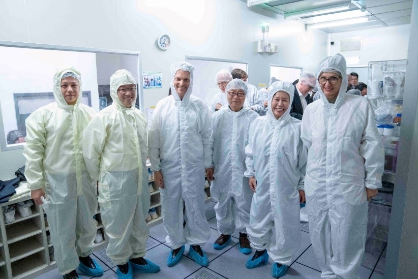
The center welcomes a delegation from Germany's Federal Ministry of Education and Research.
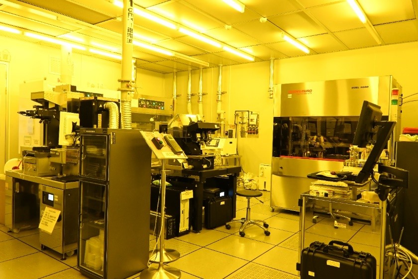
The photolithography section houses two contact aligners and a direct laser lithography system.
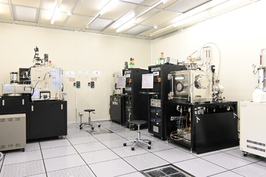
The thin film deposition section includes two e-beam evaporators and one sputter system.