The recent emergence of Gate-All-Around (GAA) technology has attracted significant attention due to its relevance in addressing the challenge of shrinking transistor sizes for the 3-nanometer semiconductor technology node. GAA technology enhances the gate's control over electric current by completely enveloping the electrical channel. It introduces a nanowire/nanosheet field-effect transistor architecture to boost performance. The transistor design has evolved from planar to now three-dimensional, transitioning from the fin-shaped structure to a multi-wire/multi-sheet configuration, aiming to maintain performance and enhance current flow while reducing size.
At the most prominent electronic device conferences, IEDM and VLSI, Professor Chee Wee Liu from the NTU Graduate Institute of Electronics Engineering (GIEE) has published a significant number of papers. He has authored 31 IEDM papers and 18 VLSI papers. Notably, his 2021 VLSI paper was selected as a highlight paper and featured in the Nature Electronics Research Highlight (NTU Newsletter Issue 1491, NTU HIGHLIGHTS No. 87). Furthermore, his 2021 IEDM paper received the prestigious Roger A. Haken Best Student Paper Award, marking a first for a Taiwanese student (NTU Newsletter Issue 1550). At the latest 2023 IEEE Symposium on VLSI Technology, Tsmc presented 6 papers, and Prof. Chee Wee Liu's group presented 5 papers with the first authors being his students(one first author co-supervised by Prof. Min-Hung Lee from Graduate School of Advanced Technology). These achievements at this year's VLSI symposium set a record for educational institutions in Taiwan.
Recently, Professor Liu's pioneering and world-leading research has yielded three significant outcomes: (1) Integration of extremely high-κ gate stacks with highly stacked channels [1] (see Figure 1); the transistor drive current sets the world record. (2) Development of the world's first standard a-IGZO GAA nanosheet FET [2] (see Figure 2). (3) Utilization of superlattice HZO grown on the n+Ge structure [3] featuring a high 2Pr of 73μC/cm2 and a high 2Ec of 5.8MV/cm, successfully create the world's first stacked GeSi nanosheet FeFET [4] (as shown in Figure 3), exhibiting a large memory window of 1.8 V at a low write voltage of 2 V.
[1] DOI: 10.23919/VLSITechnologyandCir57934.2023.10185327
[2] DOI: 10.23919/VLSITechnologyandCir57934.2023.10185385
[3] DOI: 10.23919/VLSITechnologyandCir57934.2023.10185233
[4] DOI: 10.23919/VLSITechnologyandCir57934.2023.10185284
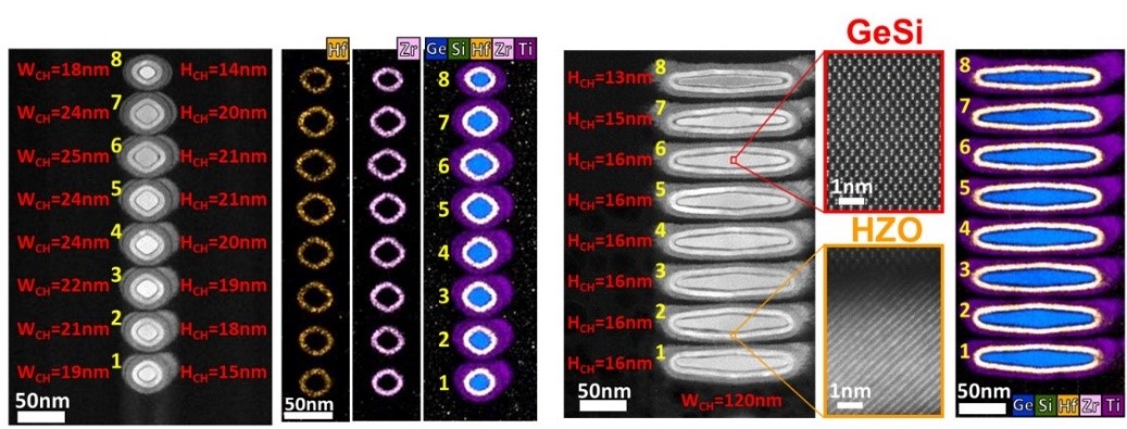
Successful integration of extremely high-
κ Hf
0.2Zr
0.8O
2 gate stacks with 8 stacked GeSi nanowires and nanosheets. The GAA structure was confirmed with EDS mappings. (©2023 JSAP)
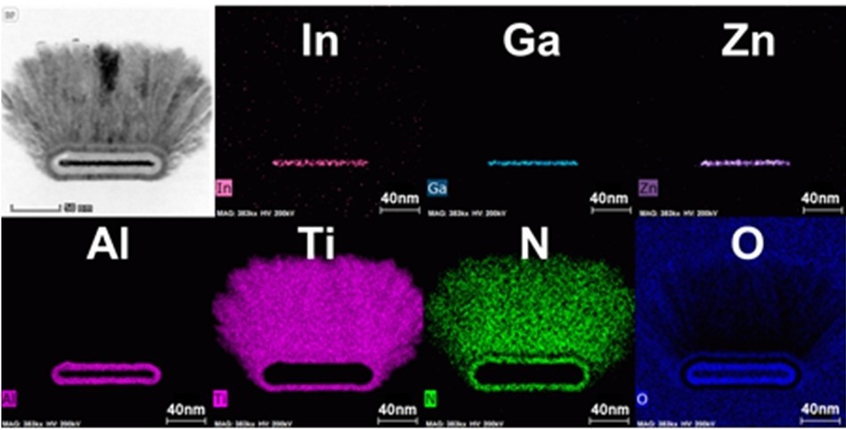
Achievement of the world's first standard a-IGZO GAA nanosheet FET. The GAA structure was confirmed with EDS mappings. (©2023 JSAP)
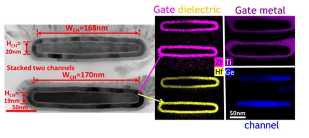 Successful creation of the world's first 2 stacked GeSi GAA nanosheet FeFET. The GAA structure was confirmed with EDS mappings. (©2023 JSAP)